Additional information
| Diameter | 2”, 3”, 4”, 5”, 6”, 8”, 12” |
|---|---|
| Wafer Type | UV Grade FS – JGS1, Optical Grade FQTZ – JGS2, Full Spectrum FS – JGS3 |
| Thickness Range | 100+ (2”, 3”, 4”); 300+ (6”); 400+ (8”); 500+ (10”,12”) |
| Finish | SSP, DSP |
Learn More
| OR | |
|---|---|
| Place Order Here | |
We accept Visa, MasterCard & American Express |
|
| Product Properties | |
|---|---|
| Product Name | Fused Silica (FS)/Quartz (FQTZ) Wafers |
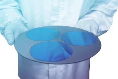
| Description | MSC offers high quality “Fused Silica” and “Fused Quartz” wafers from 2” to 12” in diameter. Fused silica is the amorphous phase of SiO2 while Fused silica is it’s pure version. Fused silica has higher transmission in the infrared and ultraviolet spectrum when compared to regular glass. We offer fused silica and quartz wafers in the following flavors: |
| Fused Silica | JGS1, UV grade: These wafers high transmission in the UV and visible spectrum (~90%). The reflection losses fall to zero between wavelengths of 150-220nm. In the infrared range, the relatively high OH concentration causes absorption for wavelengths greater than 1.2µm. |
| Fused Quartz | JGS2, Optical grade: Compared to JGS1, these wafers are cheaper and the transmission is shifted to longer wavelengths. In the UV spectrum, absorption occurs at wavelengths less than 270nm. In the visible and infrared spectrum, the low OH concentration leads to 90% absorption upto wavelengths of 2µm. |
| Fused Silica | JGS3, Full spectrum grade: These wafers offer high transparency (> 80% owing to very low OH content) over a broad spectral range of 200nm – 3µm. This peaks to 90% in the spectral range of 250nm to 2.5µm. |
| Availability | Prime wafers only. Following are some standard wafer thicknesses used: |
| Wafer Diameter | 2” – 500+/-25µm; 3” – 500+/-25µm; 4” – 500+/-25µm; 6” – 500+/-25µm; 8” – 500+/-25µm. |
| Wafer Thickness | Wafer thickness of 500 +/-25 µm is quite standard. |
| Diameter | 2”, 3”, 4”, 5”, 6”, 8”, 12” |
|---|---|
| Wafer Type | UV Grade FS – JGS1, Optical Grade FQTZ – JGS2, Full Spectrum FS – JGS3 |
| Thickness Range | 100+ (2”, 3”, 4”); 300+ (6”); 400+ (8”); 500+ (10”,12”) |
| Finish | SSP, DSP |